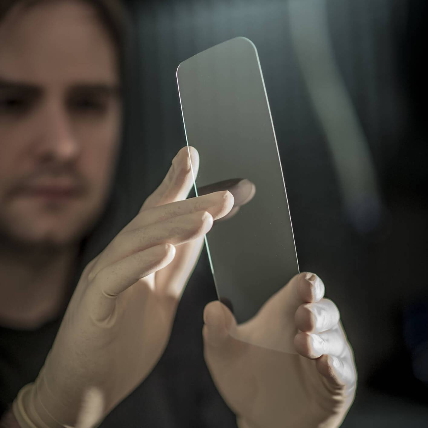
Thanks to innovative post processing, the properties of glass are immense: chemically inert, extremely temperature-resistant, heat-repellent, flexible, break-resistant, conductive... and this opens up ever new applications for glass as a material in facade glass, photovoltaic modules, consumer electronics and semiconductors, medical technology and transportation.
4JET focuses on solutions for laser-based cutting of glass and structuring of thin films on glass surfaces. We work with industry leaders to enable better products, digital production methods and sustainable manufacturing processes.
Laser Structuring
Coatings on vehicle windows, facade glass or photovoltaic modules can be removed precisely, dust-free, dry and without residues using laser technology. Our solutions enable the processing of conductive layers and thermal protection layers on flat or curved glass substrates. TCO layers such as indium tin oxide, semiconductors and metallic layers can be ablated.

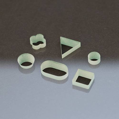
Laser Cutting
Glass components in almost any shape, with perfect edge quality and precision in the micrometer range are made possible by our PearlCut technology. Our solutions for filament cutting of glass are used in the production of displays, smart windows, sample carriers in medical technology and the separation of glass wafers. The process is suitable for soda-lime, borosilicate and chemically strengthened glasses, flexible glass foils, stacks and a wide variety of coatings.

Laser Drilling
Our solutions enable drilling of via holes and internal contours in glass components by filamentation or ablation. Depending on the required productivity, edge quality and the aspect ratio, perfect cutouts in almost any shape can be produced by combining processes. From cable feedthroughs in the cover glass of a PV module to microvias in glasses for microelectronics.

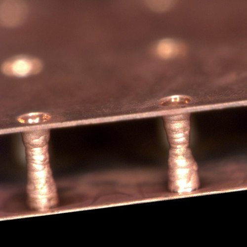
Glass volume structuring with VLIS
Our technology for the production of through-glass-vias developed together with Plan Optik AG, enables the production of metallized through-hole contacts in glass semiconductor rates. Application areas include advanced packaging, display industry, glass-based MEMS, microfluidics or high-frequency antenna technology (e.g. 6G).


